A Q&A with two scientists aiming to beat limits in computing energy and vitality effectivity by designing new microchips.
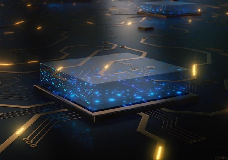
Our laptops and smartphones are compact but highly effective due to silicon microelectronics, also called microchips or chips, the tiny brains behind the digital brawn of virtually each trendy gadget.
However such trendy comfort comes at a value. By 2030, about 25% of the world’s vitality – most of which is produced by burning carbon-rich fossil fuels – could possibly be consumed by digital units if nothing is finished to make them extra vitality environment friendly.
Silicon chips originate from a design referred to as CMOS, shorthand for complementary metal-oxide-semiconductor. As Moore’s Legislation first predicted in 1975, CMOS silicon chips are approaching limits in miniaturization and efficiency. For many years, scientists have been on the hunt for brand spanking new digital supplies that transcend the boundaries of Moore’s Legislation in addition to the constraints of silicon CMOS chips.
Now, scientists Maurice Garcia-Sciveres and Ramamoorthy Ramesh at DOE’s Lawrence Berkeley Nationwide Laboratory (Berkeley Lab) are designing new microchips that would carry out higher – and require much less vitality – than silicon. Over the following three years, they may lead two of the ten initiatives lately awarded practically $54 million by the Division of Vitality to extend vitality effectivity in microelectronics design and manufacturing.
They talk about their initiatives on this Q&A.

Berkeley Lab scientists Maurice Garcia-Sciveres (left) and Ramamoorthy Ramesh are designing new microchips that would carry out higher – and require much less vitality – than silicon. Credit score: Courtesy of Garcia-Sciveres and Ramesh
Q: Over the following 3 years, what do you hope to realize? What's the significance of your work?
Garcia-Sciveres: Our undertaking – the “Co-Design and Integration of Nano-Sensors on CMOS” – goals to enhance efficiency by integrating tiny mild sensors made with nanomaterials into a standard CMOS (complementary metal-oxide-semiconductor) built-in circuit. (A nanomaterial is matter designed at an ultrasmall scale of a billionth of a meter.)
CMOS chips are manufactured from silicon, however in the event you take a look at how a lot energy silicon makes use of, it’s beginning to be important – and in a decade, silicon chips will probably be consuming a big fraction of our vitality. For instance, the computing wanted to run a self-driving automobile consumes important vitality in comparison with the vitality wanted to run the automobile. We have to compute with much less vitality, or enhance efficiency with out extra energy, however you possibly can’t try this with silicon chips as a result of silicon has to run on a sure voltage – and people bodily limitations are costing us.
In our undertaking, nanomaterials resembling carbon nanotubes – units so small that they're invisible to the bare eye – would function mild sensors. The nanosensors add new performance to a CMOS chip, rising efficiency.
Sensing is an effective preliminary utility, however when built-in right into a chip, the carbon nanotubes may additionally function transistors or switches that course of knowledge. Integrating many carbon nanotubes right into a silicon chip may result in new sorts of digital units which can be smaller and quicker in addition to extra vitality environment friendly than present applied sciences.
Ramesh: In our undertaking, “Co-Design of Extremely-Low-Voltage Past CMOS Microelectronics,” we plan to discover new bodily phenomena that can result in considerably increased vitality effectivity in computing. That is necessary as a result of we consider that the following Moore’s Legislation is more likely to be centered on the vitality scale and never the size scale, since we're already on the limits of size scaling.
In round 2015, vitality consumption from microelectronics was solely about 4-5% of the world’s complete major vitality. Major vitality sometimes means the chemical vitality produced by a coal- or pure gas-based energy plant. This sometimes has an effectivity of conversion to electrical energy of 35-40%.
Our rising reliance on synthetic intelligence, machine studying, and IoT – or the Web of Issues the place all the things is electronically linked, resembling our visitors programs, emergency response programs, and renewable vitality and electrical grid programs – will result in an exponential enhance of electronics from the programs perspective.
Because of this by 2030, vitality consumption from microelectronics is projected to be at the least 25% of major vitality. Subsequently, making electronics extra vitality environment friendly is an enormous deal.
For our undertaking, we're asking, “What basic supplies improvements may considerably cut back the vitality consumption of microelectronics?” We’re taking a look at a completely completely different framework that explores new physics utilizing a co-design strategy, through which world-leading consultants in supplies physics, gadget and circuit design, fabrication and testing, and chip-level structure are working in collaboration to hold out a holistic examine of pathways to next-generation computing.
Q: What new functions will your work allow, and the way will you display these new capabilities?
Garcia-Sciveres: Our work will display a single-photon imager that may measure the spectrum – the wavelength or vitality – of each single photon or mild particle it detects. This enables for hyperspectral imaging – that's, photos the place every pixel may be decomposed into many colours, offering rather more info. Hyperspectral imaging advantages a broad vary of science, from cosmology to organic imaging.
The Darkish Vitality Spectroscopic Experiment (DESI), a world science collaboration managed by Berkeley Lab, captures the spectra of distant galaxies, ranging from photos of the galaxies that have been beforehand taken with different devices. This added spectral info helps cosmologists perceive how darkish vitality formed the growth of our universe. Had the unique observations of the galaxies been made with a hyperspectral imager, spectral info would have been accessible to start with.
One other rising utility of hyperspectral imaging is the examine of exoplanets. (Planets in our photo voltaic system orbit across the Solar. Planets that orbit round different stars are referred to as exoplanets.)
However the sensors used for a majority of these observations work at temperatures lower than 1 diploma above absolute zero. Our gadget would work at extra sensible temperatures, maybe even as much as room temperature.
Hyperspectral imaging has many functions in drugs and biosciences, and plenty of business devices can be found. Nonetheless, these devices, that are all rather more complicated and costlier than an everyday digicam, both scan an object pixel by pixel or have complicated preparations of robotic fibers or filters. Furthermore, these devices would not have single-photon sensitivity. Our gadget would allow a easy digicam that gives hyperspectral photos with single-photon sensitivity.
Ramesh: Our workforce is designed to display the viability and energy of our co-design platform, “Atoms to Structure,” which is constructed upon two basic bodily phenomena:
The primary is a novel conduct in ferroelectric-based transistor architectures that gives a pathway to scale back the entire vitality consumed in a silicon-based microelectronics gadget. (A ferroelectric is a cloth with an electrical dipole – or a pair of constructive and adverse electrical fees – that's switchable with an electrical discipline.) The second is the low-voltage electrical discipline manipulation of digital spin utilizing a novel class of supplies referred to as multiferroics.
In 2014, we demonstrated a magneto-electric materials that may convert cost into magnetic spin at 5 volts of utilized voltage. Subsequent collaborative work with researchers at Intel confirmed how this could possibly be used to create a brand new class of logic-in-memory units, termed the MESO gadget, which makes use of spins to hold out logic operations.
For one in every of our initiatives inside our program, we are going to use our magneto-electric materials to discover multiferroic parts that can perform at 100 millivolts, resulting in a big drop in vitality consumption. (A millivolt is one thousandth of a volt.)
Our second undertaking is exploring the basic physics of a capacitor gadget, through which a ferroelectric layer is overlaid on a standard silicon transistor to reinforce its vitality effectivity by means of what’s referred to as the adverse capacitance impact. Our design would allow a microelectronics gadget that carries out each reminiscence and logic capabilities – This strategy is radically completely different from the chips in our computer systems right now, the place one type of chip performs the logic or processing of information, and one other chip shops knowledge.
The “Co-Design and Integration of Nano-Sensors on CMOS” undertaking is a collaboration between researchers at Berkeley Lab, Sandia Nationwide Laboratory, and UC Berkeley. Co-principal investigators embody Weilun Chao, Steve Holland, Mi-Younger Im, Tevye Kuykendall, Francois Leonard, Yuan Mei, Andrew Nonaka, Katerina Papadopoulou, Greg Tikhomoirov, Archana Raja, Ricardo Ruiz, and Jackie Yao.
The “Co-Design of Extremely-Low-Voltage Past CMOS Microelectronics undertaking” is a collaboration between researchers at Berkeley Lab and UC Berkeley. Co-principal investigators embody Sinéad Griffin, Lane Martin, Lavanya Ramakrishnan, Sayeef Saluhuddin, Padraic Shafer, John Shalf, Dilip Vasudevan, and Jackie Yao.
Post a Comment